Product Overview
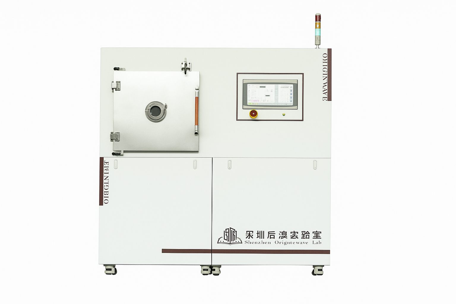
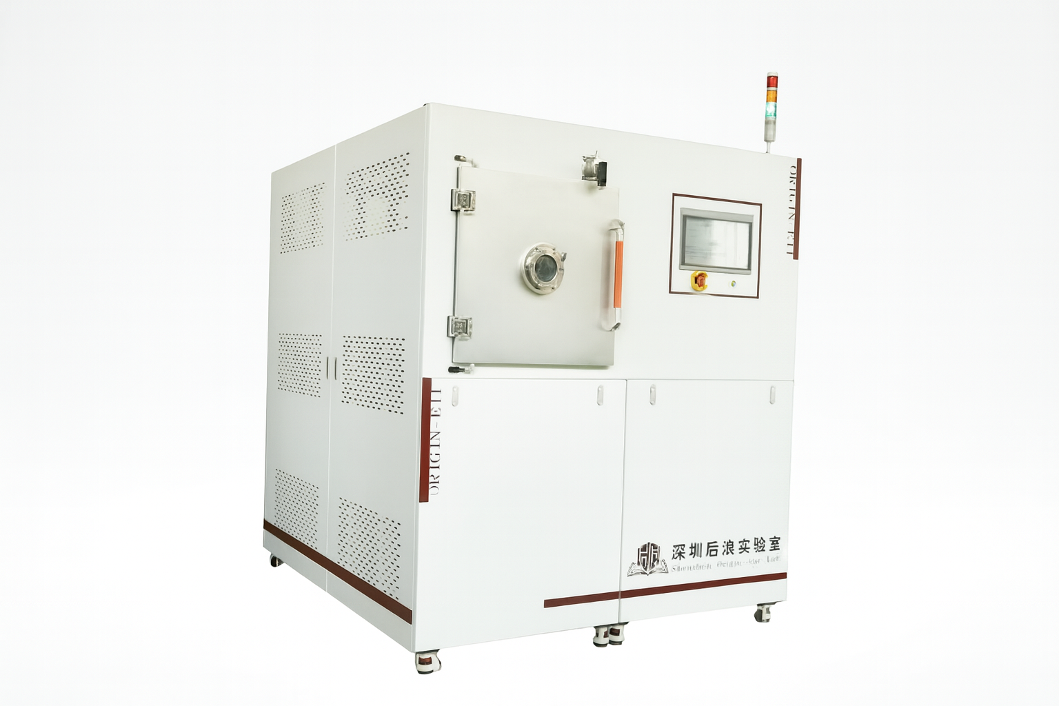
The JP-5050 is a research-grade magnetron sputtering coating system featuring a vertical front-opening structure with a chamber size of Φ500×500 mm. Designed for convenience, compactness, and easy maintenance, it is ideal for universities, research institutes, and material enterprises engaged in thin-film deposition and process development.
Key Features
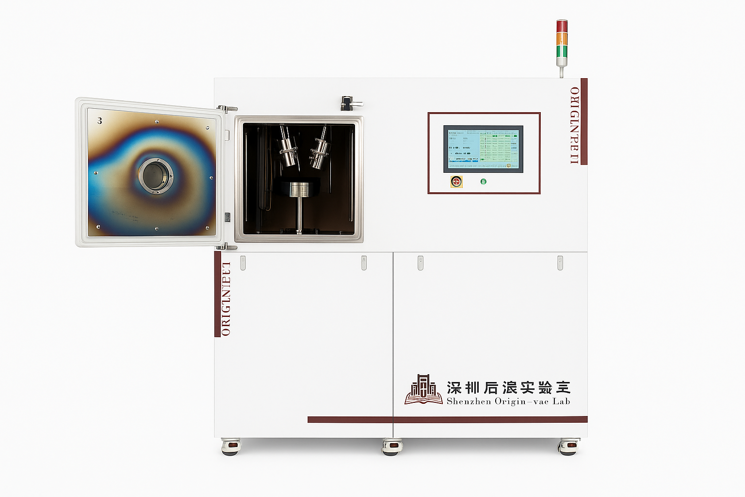
Vertical front-opening chamber for easy sample loading, cleaning, and maintenance.
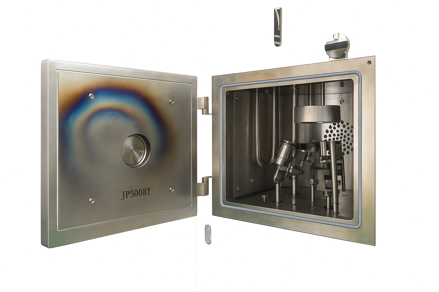
Top-mounted heated rotating substrate holder supporting revolution and multi-angle deposition, with a maximum temperature below 500 °C.
Four 2-inch planar magnetron targets with adjustable angles, compatible with DC, MF, dual-pulse, and RF power configurations.
High-performance turbomolecular pumping system providing a stable high-vacuum environment for uniform and repeatable coatings.
Fully automated PLC control system with touch screen interface for precise parameter setting, real-time process monitoring, and data recording.
Multi-material compatibility suitable for metal, ceramic, oxide, and composite film deposition.
Technical Specifications
| Specification | Parameter |
|---|---|
| Chamber Size: | Φ500 × 500 mm |
| Target Quantity: | 4 (angle adjustable) |
| Target Size: | Φ2-inch planar targets |
| Vacuum System | Turbomolecular + Mechanical pump set |
| Substrate Holder: | Heated rotating stage, temperature ≤ 500 °C |
| Power Supply Options: | DC / MF / Dual-pulse / RF |
| Control System: | PLC + touch screen automation |
| Ultimate Vacuum | 5×10⁻⁵ Pa (or better) |
Application Fields and Typical Coatings
Semiconductor and Microelectronics
Application: Adhesion layers, diffusion barriers, seed layers, backside metallization, and packaging metals.
Typical Films: Ti/TiN, Ta/TaN, W, Cu, Al, NiV/Cu, Pt, Au, SiO₂, SiNx.
Value: Enhances interconnect reliability, reduces contact resistance, and improves chip yield.
Display, Touch, and Optoelectronic Devices
Application: Transparent conductive layers, back electrodes, and barrier layers.
Typical Films: ITO, AZO, Mo/Al/Mo, SiNx.
Value: Improves light transmittance and conductivity, extending OLED/μLED device lifetime.
Optical and Laser Coatings
Application: Anti-reflection, high-reflection, beam-splitting, bandpass, cutoff, IR window, and hard coatings.
Typical Films: SiO₂, Al₂O₃, TiO₂, Ta₂O₅, Nb₂O₅, Cr, Al, Ag.
Value: Achieves desired spectral properties, high laser damage threshold, and excellent surface hardness.
Magnetic and Spintronic Materials
Application: Soft/hard magnetic layers, GMR/TMR multilayers, and magnetic sensors.
Typical Films: NiFe, CoFe, Co/Ni superlattices, Ru, MgO.
Value: Enables development of high-sensitivity magnetic sensors and spintronic devices.
MEMS and Sensors
Application: Electrodes, resistive/thermal/strain layers, and piezoelectric thin films.
Typical Films: Pt, Au, Ti, AlN, ZnO.
Value: Provides stable electrical properties with low internal stress, ideal for microstructures.
New Energy and Energy Storage
Application: Photovoltaic back electrodes, transparent conductive layers, and solid-state battery functional films.
Typical Films: Mo, Ti, Al, ITO/AZO, LiPON (reactive sputtering).
Value: Improves energy conversion efficiency and enhances cycling stability.
Cutting Tools, Molds, and Mechanical Components
Application: Wear-resistant, anti-friction, corrosion-resistant, and decorative-functional coatings.
Typical Films: TiN, TiAlN, CrN, MoS₂, DLC.
Value: Extends service life, reduces friction, and minimizes maintenance costs.
Medical and Biomedical Engineering
Application: Bio-inert and antibacterial coatings, medical electrodes, and marking layers.
Typical Films: Ti, TiN, ZrN, Ag, DLC.
Value: Improves biocompatibility and enhances wear and corrosion resistance.
Automotive and Architectural Glass / Energy-saving Applications
Application: Low-E coatings, reflective and anti-corrosion layers, infrared control coatings.
Typical Films: Ag/NiCr/SiNx multilayers, Al, Cr, ITO.
Value: Provides energy-saving insulation, corrosion resistance, and customizable appearance.
Scientific Research and New Material Development
Application: Multi-element alloy co-sputtering, heterojunctions, superlattice, and multilayer/gradient film structures.
Features: Four-target co-sputtering with synchronized rotation for compositional and thickness gradient design.
Value: Enables rapid material screening and process optimization, bridging laboratory studies to pilot or mass production.